In thermal imaging, the infrared sensor is the core component. Sensor performance directly affects end-product image quality, reliability, and application range. Yet that performance is heavily shaped by packaging technology. Metal packaging, ceramic packaging, and wafer-level packaging (WLP) currently coexist in the infrared industry. This article systematically analyzes how different packaging methods affect the performance of an infrared sensor. It compares the technical characteristics and application boundaries of metal, ceramic, wafer-level, and super wafer-level packaging (SWLP). It also examines future packaging trends.
Why Packaging Matters — Four Dimensions That Directly Affect Infrared Sensor Performance
Reliability: Infrared chips are highly sensitive to moisture, dust, mechanical shock, and other external conditions. Packaging must create a stable protective barrier. It must also maintain a high vacuum to prevent chip performance degradation or failure.
Performance: The thermal conductivity of the packaging directly affects chip heat dissipation. Poor heat dissipation increases noise and reduces detection accuracy.
Integration: Package size, weight, and interface determine whether the detector meets integration requirements across different applications.
Cost: Material selection and process complexity affect mass production efficiency and unit cost. These differences significantly impact the widespread adoption of infrared thermal imaging technology.
Four Infrared Sensor Packaging Technologies: Key Features and Applications
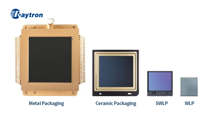
Current mainstream thermal sensor packaging methods includes metal, ceramic, wafer-level (WLP), and super wafer-level (SWLP). Each of these thermal sensor package types has distinct strengths. Each serves different application domains.
Metal Packaging: High Reliability
Metal packaging is one of the earliest thermal sensor packaging types for infrared detectors. A metal shell isolates the chip from the external environment to create a sealed, vacuum-capable protective enclosure. The typical construction includes a metal shell, thermoelectric cooler (TEC), and a cylindrical getter. The TEC stabilizes the operating temperature near room temperature, improving thermal imaging sensor performance in extreme environments.

Metal packages deliver extremely high mechanical strength, excellent thermal conductivity for heat dissipation, and strong sealing for high reliability. However, metal packaging has clear drawbacks. Metal materials are expensive, the manufacturing process is complex, and the resulting detectors remain large and heavy, limiting miniaturization.
Metal packaging is primarily suited for applications requiring maximum reliability and heat dissipation where size and weight are not critical constraints. Examples include military systems, aerospace platforms, border surveillance, and high-end industrial inspection equipment.
Ceramic Packaging: Balancing Performance and Cost
Ceramic packaging replaces the metal shell with ceramic material. It retains sufficient mechanical strength and reliability while achieving significant weight reduction and cost optimization, making it a widely adopted thermal sensor packaging type in high-end devices. The typical construction uses a ceramic substrate, infrared window, and a thin-film getter. Some designs incorporate readout integrated circuits (ROIC) with built-in temperature compensation, reducing or eliminating the need for a TEC. This allows further reduction in package size and power consumption where performance requirements permit.
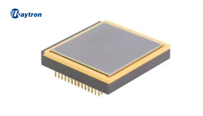
Ceramic packages offer mechanical and thermal stability comparable to metal alternatives, with sealing performance that approaches metal standards. They are significantly smaller and lighter than metal packages, enabling easier system integration. However, they remain relatively costly and complex to manufacture. The resulting dimensions are still larger than wafer-level alternatives, and stability under rapid, extreme temperature shifts falls slightly below that of metal packaging.
These characteristics make ceramic packaging well-suited for applications demanding high performance and reliability with moderate integration requirements. Typical uses include industrial automation, security and surveillance, unmanned systems, robotics, advanced driver-assistance systems (ADAS), and firefighting equipment.
Wafer-Level Packaging (WLP): Extreme Miniaturization
Wafer-level packaging represents a revolutionary breakthrough in thermal sensor packaging technology. WLP eliminates the need for additional housing by integrating the window and chip directly at the wafer stage. High-vacuum packaging is completed on the entire MEMS wafer before dicing into individual detectors. This approach consolidates most packaging and testing steps prior to wafer dicing, dramatically improving production efficiency.
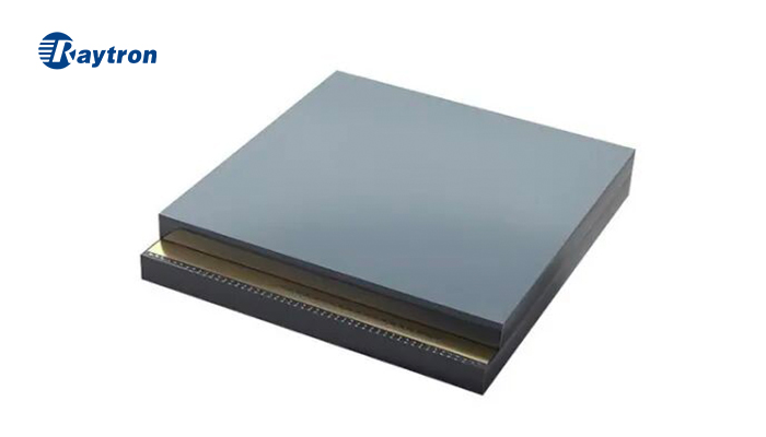
WLP achieves extreme miniaturization and light weight, with package dimensions approaching those of the chip itself. Manufacturing efficiency far exceeds traditional chip-to-chip packaging, enabling mass production at scale. By eliminating individual tube assembly and wire bonding steps, WLP significantly reduces unit cost. However, the packaging process is technically complex, post-packaging production lines require substantial fixed-asset investment, and cleanroom requirements are extremely strict.
WLP is typically used in consumer electronics, wearable devices, Internet of Things (IoT) systems, civilian drones, portable devices, and advanced driver-assistance systems where size, weight, and cost are critical.
Super Wafer-Level Packaging (SWLP): Advanced System Integration
Super wafer-level packaging is an advanced form evolved from WLP. It specifically addresses downstream integration pain points of WLP. In WLP, the chip remains exposed and vulnerable to dust, requiring complex wire-bonding and multiple dust-protection steps in a cleanroom. This creates high environmental demands, complex workflows, and limited yield. SWLP solves these issues through a new window design and double-layer packaging structure that fully encapsulates the chip internally. It directly matches SMT mounting processes without wire-bonding, enabling rapid integration in standard workshop environments.
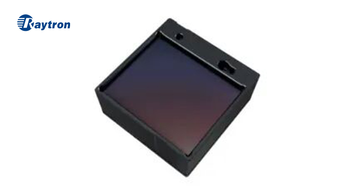
SWLP inherits the extreme miniaturization and light weight of WLP. It completes electrical signal routing without separate wire-bonding. The package provides dust and particle protection, overcoming the strict cleanroom limitations of WLP. It matches SMT technology for fast, high-volume production.
SWLP is suited for miniaturized devices sensitive to size, weight, and cost. It significantly lowers industry entry barriers, allowing more companies to independently develop and manufacture camera core modules. It is ideal for consumer electronics, wearable devices, IoT sensors, and portable systems where rapid SMT assembly and cost control are essential.
Future Trends in Infrared Sensor Packaging Technology
From traditional metal and ceramic packaging to WLP, and then to highly integrated, scalable SWLP, uncooled infrared focal plane detector packaging will continue to evolve around system-level integration, miniaturization and weight reduction, and the balance of low cost with high reliability. It will improve integration, reduce size and weight, and further expand the application boundaries of infrared technology.
Which Sensor Packaging Type is Right for Your Application?
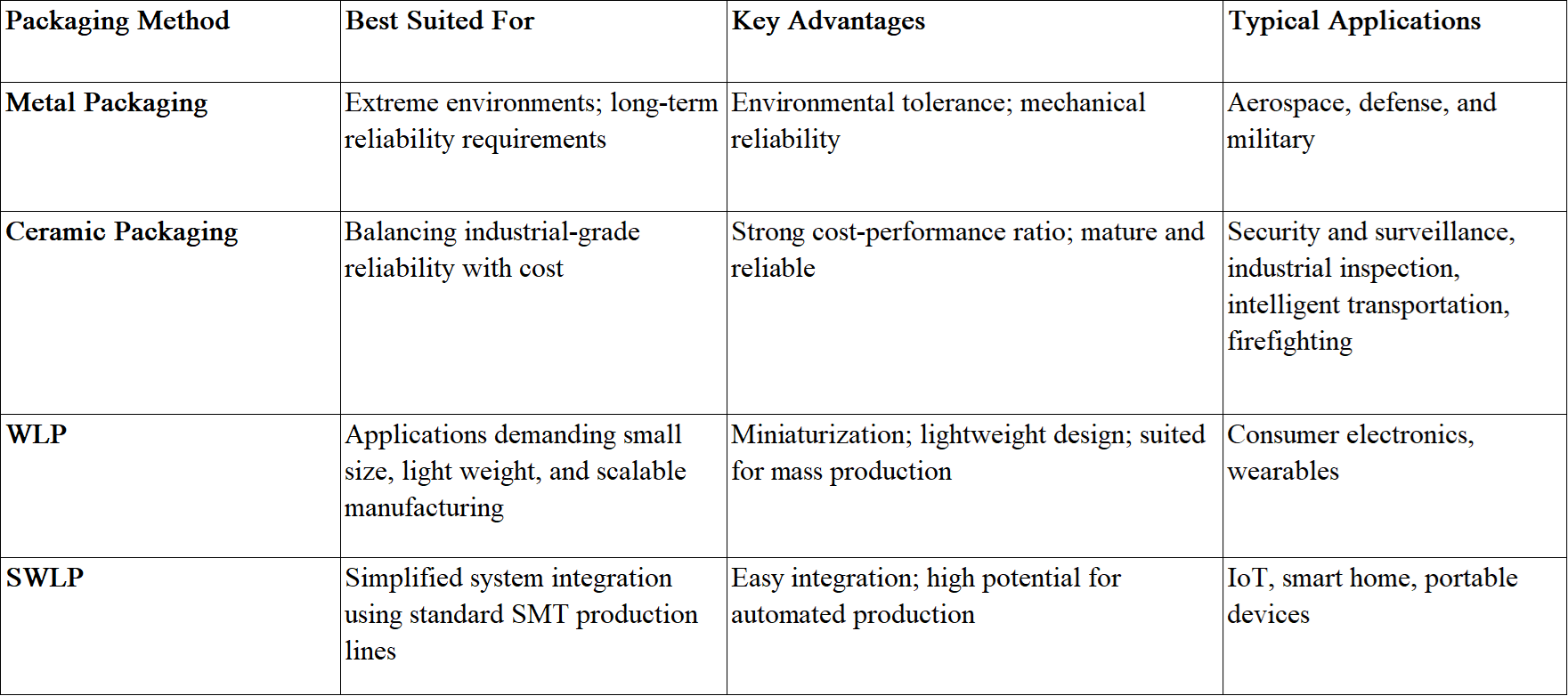
The best packaging choice depends on your application requirements. Use the quick guide below to identify the most suitable option based on reliability, size, performance, and cost.
Conclusion
Packaging technology is a critical yet often overlooked element in uncooled infrared thermal imaging. From the extreme reliability of metal packaging, to the performance-cost balance of ceramic packaging, to the mass production breakthrough of WLP, and the system integration innovation of SWLP—each packaging method delivers value in its suited applications.
For infrared sensor designers and buyers, understanding the technical characteristics, performance impact, and cost structure of different packaging methods is essential for making the correct selection. As packaging technology continues to evolve toward higher integration, smaller size, and lower cost, infrared thermal imaging is accelerating from professional fields into a wide range of industries, enabling more innovative applications.
About Raytron
Raytron specializes in uncooled infrared focal plane detectors and thermal imaging solutions. The company offers full-series packaging capabilities spanning metal packaging, ceramic packaging, wafer-level packaging (WLP), and super wafer-level packaging (SWLP). Its product line covers multiple resolutions from 256×192 to 1280×1024, with annual capacity reaching several million units. We deliver optimal SWaP-C (Size, Weight, Power, Cost) solutions through continuous packaging innovation. Whether your application requires high reliability in extreme environments or mass production at the consumer electronics level, Raytron provides suitable infrared sensor products and technical support.