Thermal imaging is expanding beyond traditional professional applications into automotive, industrial, consumer electronics, robotics, and other markets. As the technology evolves, a leading thermal camera brand needs more than strong individual specifications—it needs proven technology, scalable manufacturing, and market validation. This article examines these three proof points and how Raytron is strengthening its position through continuous innovation, mass production, and real-world customer adoption.
Technology Proof: The Technology Behind Leading Thermal Camera Brands
For a leading infrared thermal imaging manufacturer, competitive strength goes beyond the imaging performance of the final product. It also depends on control of the underlying technology chain.
From 8 μm to 6 μm: Breaking New Ground in Detector Pixel Pitch
One major trend in infrared detector development is to reduce pixel pitch while maintaining performance. Smaller pixel pitch increases pixel density and enables higher-resolution imaging in more compact form factors. Raytron has developed the world's first 8 μm 1920 × 1080 uncooled infrared detector and the world's first 6 μm 640 × 512 uncooled infrared detector, continuing to advance uncooled infrared detector technology toward smaller pixel pitches.
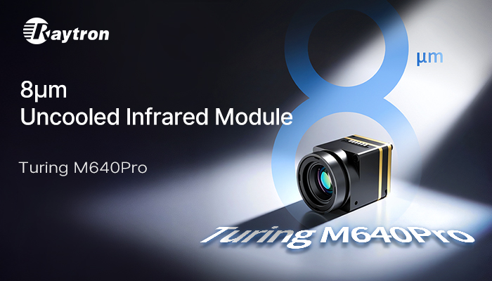
A smaller pixel pitch enables higher spatial sampling density within the same detector size. It also creates more room for compact optical systems and smaller end products. This is important for expanding thermal imaging into applications such as automotive systems, consumer electronics, and robotics, where size and integration are increasingly important.
Industry-First SWLP Packaging
Packaging is an important factor in determining the size, reliability, power consumption, and manufacturing efficiency of infrared detectors.
Traditional metal and ceramic packages offer proven reliability, but there is still room to optimize their size, weight, and manufacturing cost. Wafer-level packaging (WLP) provides another path toward smaller infrared detectors and more efficient mass production.
Building on this approach, Raytron has developed SWLP technology. Its dual-layer package design improves resistance to particles and dust in assembly environments and supports efficient SMT mounting. This creates more opportunities for thermal imaging to be integrated into smartphones, automotive systems, robotics, and other compact intelligent devices.
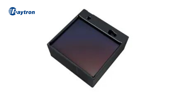
The combination of 8 μm and 6 μm pixel-pitch technologies with SWLP packaging enables infrared detectors to achieve higher pixel density in smaller form factors, while supporting greater integration at the end-product level. These underlying technology advances are helping thermal imaging move beyond traditional professional equipment toward more compact and intelligent products for automotive, consumer electronics, robotics, and other applications.
Overall, Raytron's technology capabilities extend beyond individual device performance to cover detector design, MEMS, ROIC, packaging and testing, image algorithms, and system integration. As of the latest publicly reported period, Raytron had filed 3,824 intellectual property applications and received 2,391 grants [Source: Raytron Technology Co Ltd’s 2025 Annual Report]. This continued investment in R&D and intellectual property provides a foundation for ongoing innovation in infrared thermal imaging technology.
Scale Proof: From Innovation to Mass Production
Technical breakthroughs create commercial value only when they can be translated into stable, consistent, and cost-effective mass production. For a thermal camera brand, developing a prototype is only the first step. The real test is whether detectors, modules, and complete imaging systems can be brought into stable mass production while maintaining consistent product quality and supply.
Raytron has established a manufacturing system covering infrared detectors, wafer-level packaged products, and complete imaging systems. Its infrared detector manufacturing platform has an annual capacity of 6 million units, while its wafer-level thermal imaging module manufacturing capacity exceeds 5 million units per year. Its annual capacity for complete thermal cameras has reached the million-unit level [Source: Raytron Technology Co Ltd’s 2025 Annual Report]. This manufacturing system, spanning detectors, modules, and complete systems, enables Raytron to translate technological innovation into stable volume supply and support product demand across automotive, industrial, outdoor, consumer electronics, and other markets.
Market Proof: Global Customer Adoption and Market Recognition
Technology and manufacturing capacity ultimately need to be validated by real customers and production programs. For a leading thermal camera brand, market recognition is not simply about products being purchased. It also means that core technologies can meet the reliability and engineering requirements of real-world applications.

Automotive OEM
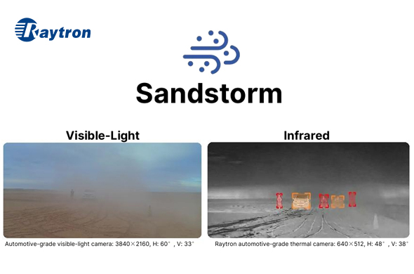
Automotive is an important market for validating the engineering capabilities of infrared sensing technology. Raytron's automotive infrared technology has passed relevant AEC-Q100 qualification and continues to advance the mass production of automotive thermal imaging solutions for intelligent driving and active safety applications.
Raytron currently works with more than 20 automotive OEMs, including BYD, Great Wall Motor, Geely, Didi, and Dayun, supporting more than 30 vehicle models. Raytron also works with Breiton, known as the “first listed company focused on zero-carbon mining robots,” where infrared thermal imaging and 4D millimeter-wave radar provide complementary sensing for autonomous mining trucks. In 2026, the Zeekr 9X achieved the world's first production implementation of thermal AEB (Automatic Emergency Braking), marking the integration of infrared technology into the core safety control chain of intelligent driver-assistance systems.
Industrial Customers
In industrial applications, thermal imaging is widely used for predictive maintenance, electrical inspection, equipment condition monitoring, and high-temperature measurement. Raytron continues to advance infrared temperature measurement technologies for high-temperature industrial processes, supporting applications in metallurgy, power, and other industries.
Beyond temperature measurement, infrared-based solutions are also used in emergency response, energy infrastructure, and oil and gas storage and transportation. By enabling non-contact temperature monitoring and providing complementary visual information, these technologies can support equipment inspection and situational awareness in complex operating environments.
International Customers
From core infrared detectors to modules and complete systems, Raytron continues to expand its global market presence, providing further application validation for its infrared technologies in international markets. Today, Raytron's comprehensive portfolio of products and solutions serves customers across Asia, North America, Europe, South America, Oceania, and Africa, with a marketing network covering more than 100 countries and regions and providing products and solutions to customers worldwide.
Conclusion: FromThermal Imaging to Intelligent Sensing
Thermal imaging is evolving from a standalone imaging technology into more compact, power-efficient, and intelligent sensing solutions. As infrared, visible light, radar, laser, and other sensing technologies become increasingly integrated, future infrared sensing solutions will place greater emphasis on multi-sensor coordination and system-level integration, providing richer environmental information for intelligent systems in automotive, robotics, industrial, and other applications.
Raytron has established competitive strengths across technology development, mass production, market validation, and application experience in infrared thermal imaging. At the same time, the company has been laying the groundwork for AI-powered sensing technologies, integrating infrared, microwave, and laser with AI capabilities to address the evolving requirements of next-generation intelligent sensing.
About Raytron
Founded in 2009, Raytron is committed to becoming a leading global supplier of core components and subsystems for multimodal sensing. The company focuses on infrared, microwave, and laser sensing technologies, with a product portfolio spanning chips, detectors, modules, and complete systems. With end-to-end capabilities from chip design to system integration, Raytron continues to advance intelligent sensing through technological innovation and mass production.